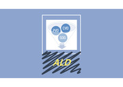
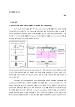
/advances-in-atomic-layer-deposition-of-semiconductor-device-2/ Spatial Atomic Layer Deposition (SALD ... ALD ALD (Atomic Layer Deposition) ALD 공정 개요 다양한 기재 (substrate) 위에 금속 전구체와 반응 가스를 교차적으로 주입 ↓ Self-limiting ... Atomic layer deposition) ALD 최근 기술 동향 기존의 ALD : Precursor 가 기판에 접촉하는 면적 , 위치 제어 불가능 ↓ AS-ALD : 전구체 (
using directed-energy deposition. ... Also, I will study about Design of 2D Layered Catalyst by Coherent Heteroepitaxial Conversion for Robust ... , I will study about Electronic Promotion of Methanol Synthesis over Cu-Loaded ZnO-based Catalysts, Atomic
deposition (CVD) is one of the mapproximately 50% of the total wafer-processing time. ... In ion implantation, dopant atoms are forcefully introduced into silicon in the form of an energetic ... Generally, it involves the movement of dopant atoms into silicon through thermal processes in a furnace
surface 4-2.)E-beam evaporation A method of ionizing the deposited atoms or molecules and accelerating ... Therefore, it is necessary to form a very thin layer of a material having electrical characteristics, ... The process of silvering was once commonly used to produce mirrors, while more recently the metal layer
thin-film transistors through controlled crystallization, High-Performance Thin-Film Transistors with an Atomic-Layer-Deposited ... as a highly efficient electrocatalyst for oxygen reduction reaction, Effect of the Particle Size and Layer
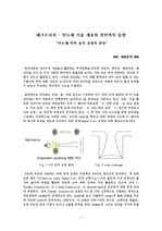
제목 차세대 배선 재료로서 고품질 루세늄 박막에 대한 플라즈마 강화 원자층 증착(Plasma-Enhanced Atomic Layer Deposition, PEALD) 공정 개발 II ... 새로운 재료들을 배선공정에 사용하기 위해서는 대표적으로 PEALD (Plasma Enhanced Atomic Layer Deposition) 증착 법을 이용하였다. ... 2022학년도 1학기 재료공학캡스톤디자인(1) 1차 개인보고서 차세대 배선 재료로서 고품질 루세늄 박막에 대한 플라즈마 강화 원자층 증착(Plasma-Enhanced AtomicLayer
vapor 혹은 sputtered atom을 substrate로 이동시킨다. 3) substrate의 표면 위에서 coating vapor 혹은 sputtered atom을 응축시킨다 ... Thin-film Deposition Techniques Physical Vapor Deposition PVD는 주로 evaporation과 sputtering으로 나누어진다. ... Electrochemical Deposition 두께가 두꺼운 막을 증착시키는 데 필요하다.
물질 증착 기술인 ALD(Atomic Layer Deposition) 방법을 이용하여 Si/SiO2 기판 및 Powder 등 다양한 물질에 Pt, Ru, W 등 여러 물질을 증착하여 ... LayerDeposition) Lab, and Accelerator. ... attached resume, I have various experiences such as International Conformity Expert Training, ALD (Atomic
using ALD (Atomic Layer Deposition). ... 반도체 스터디를 통해 깨닫게 된 것은 Thin Flim Deposition에 흥미를 느끼고 있다는 것이었습니다. ... 이를 통해 제가 하고 싶은 Thin Flim Deposition에 대해 연구하기 위해서는 대학원에서 전문성을 키워야 한다고 생각합니다.
Fig. 4 ALD 공정 형태 마지막으로 반도체 제조에 주로 사용되는 세 번째 공정은 ALD(atomic layer deposition) 공정(Fig.4)으로 기존 PVD, CVD의 ... deposition) 공정에 대해 알아보고자 한다. ... 또한, 이 과정은 원하는 layer의 층만큼 반복될 수 있다.
LayerDeposition 등이 있다. ... 얇은 반도체 thin film이나 layer의 전기 저항을 sheet resistance라 한다. ... 박막을 형성하는 기술로서PECVD(Plasma Enhanced), LPCVD(Low Pressure), APCVD(Atmospheric Pressure), thermal CVD, Atomic
On increasing the substrate temperature on depositing the buffer layer on the silicon substrate, shorter ... barrier because the diffusion barrier prevents generation of silicon carbide from the diffusion of carbon atoms ... For synthesizing vertically aligned carbon nanotubes, thermal chemical vapor deposition is used and a
LayerDeposition [as aspect ratio goes high conventional CVD cannot be possible -> ALD/ALE] CLEANING ... surface diffusion f) incorporation into the crystal lattice g) desorption h) gas phase diffusion Ks Atomic ... Free Path : a지점에서 b지점 충돌 후 다시 b지점 돌아올 때 가지의 확률 For high MFP : 진공(압력 low), 기체분자 low [압력을 낮추기 위해 pump사용] Deposition
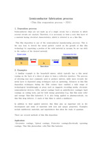
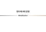
LayerDeposition) 화학 반응에 의해 원자가 떼어지는 것을 이용 , 한 층씩 쌓는 방식으로 증착 Method 장점 단점 PVD 저온 증착 가능 모든 물질 증착 가능 불순물 ... Plasma Enhanced CVD) : 저온 (400 ℃) 에서 플라즈마를 이용해 분해시켜 표면에 증착 ( 고온으로 올라가면 금속이나 Si 기판이 녹을 우려 ) Method ALD(Atomic ... Silicide Process Materials Structure Method Reference 8 대 공정 요약 Wafer Oxidation Photo Lithography Etching Deposition
layer thickness over an area of about 125 × 125 mm. ... The surface of carbon films deposited with inverted plasma fireballs is analysed in this paper. ... Measurements were conducted with Raman spectroscopy, atomic force microscopy and nanoindentation.
Plasma Enhanced Chemical Vapor Deposition (PECVD) Pdeal components are shown by the dotted line. ... A conjugated system is formed where carbon atoms covalently bond with alternating single and double bonds ... Table 5 shows the key parameters of the devices with different active layer composition.