Remote plasma-enhanced CVD (RPECVD) - 와이퍼를 플라즈마와 분리하여 룸템퍼레츄어에서 가능하도록 만든 PECVD - 나머지 여러가지 : Atomiclayer ... precursor layers on the desired substrate ③ 열처리 : deposited layer를 의도된 desired crystallize phase로 바꿈 ... Thin film deposition : layers of insulators, semiconductors, and conductors form integrated circuit 등을
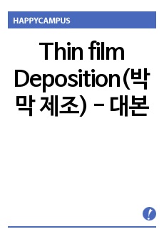
LayerDeposition technique을 사용한 방법 Silicon-on-insulator using stress limited oxidation에서의 생성법등 많은 방법이 ... 하지만 SLS방법의 단점은 낮은 온도에서 진행이 되기 때문에 atom의 이동도가 떨어져서 합성된 나노와이어의 결정성이 낮을수 있다는 점이다. ... Laser ablation method, 등의 방법이 있으며 Anodic Aluminum Oxide (AAO) template method, AAO 와 VLS 법을 혼합한 방법 Atomic
둘째, 다공성 지지체의 기공내에 박막이 형성되는 경우 기공이 완전히 막히지 않고 작은 구멍(pin-hole)이 생길 수도 있다. 2) ALD (원자층 증착법, AtomicLayer ... 증착표면 근처에서는 기체흐름이 가열되고, 점성에 의해 속도가 떨어지며, 조성의 변화가 생기기 때문에 열, 운동량, 화학조성의 boundary layer가 형성된다. ... Deposition) ALD공정은 purge에 의해 기판 표면에 한 층만 남아서 반응에 참여하게 되므로 다른 공정변수의 의존도가 적으며, 박막의 두께는 cycle수에만 의존하게 된다
따라서 최근에 이러한 물리적 증착법의 한계를 극복put위한 대안으로 화학기상증착법(CVD) 혹은 원자층 증착법(atomic layer deposition : ALD)에서젠기되고 있다 ... 발명의 목적과 그 핵심은 anode인 ITO와 Hall transport layer 간에 계면저항을 줄여서 hole의 주입 효율을 향상시키는 것이다. ... 기존에 사용된 Pure ITO의 work function은 4.6 eV로 Hall transport layer로 사용되는 CuPc와 큰 차이를 보인다.
Au(111)(a) and the modified gold surface Au(111) with 1,4-dithiane after 72h of immersion time (b) Layer에는 ... 생명·분자공학부 200421808 김경해 200421887 허지호 나노 기술 입문 Contents Definition of AFM Principle of AFM Atomic force ... Deposition process of monomolecular films on solid substrate What is Langmuir-Blodgett film?
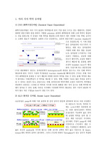
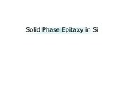
Definition : a special case crystal growth in which a single crystal face grows by the addition of atoms ... 100) Oxide Si(100) Oxide α-Si Si(100) Oxide α-Si Schematic Diagram of Lateral Solid Phase Epitaxy As deposited ... 1st Amorphous layer 1st Crystal layer 2nd Crystal layer Model for the interface of amorphous-crystal
응용분야 진공 플라즈마 시스템을 이용하는 응용분야로써 일반 반도체 공정에서 사용되는 건식 식각 공정, 증착 공정, 에싱(ashing) 공정, ALD(Atomic Layer Deposition ... 활발한 플라즈마는 저온 글로우 방전 플라즈마로서 반도체 공정에서 플라즈마 식각(plasma etch) 및 증착 (PECVD: Plasma Enhanced Chemical Vapor Deposition
), 단원자층 화학기상증착(ALCVD: AtomicLayer Chemical Vapor Deposition)등의 공정을 통해 만들어진다. ... 칼코게나이드(GST) 박막은 고진공 하에서 화학기상증착(CVD: Chemical Vapor Deposition), 플라즈마 화학기상증착(PECVD: Plasma Enhanced CVD
Figure 5.1 Cluster는 작은 노즐을 통해서 진공 공간으로 단열 팽창해 나갈 때 super saturated vapor atom의 응축에 의해 형성된다. ... Table 1.1 A classification of the film deposition PVD (physical vapor deposition) CVD (chemical vapor ... Film layer의 위의 표면과 아래 바닥에서 어떻게 반사되는지의 관계를 기초로 해서 reflectometry는 film 두께를 계산할 수 있다.
invasion Bandgap disappear Metallic compound Pin hole Mg-Ag TCO Sputtering (Organic layer degradation ... by heat energy C H Short Short Bandgap disappear Metallic compound Bonding destruction Energetic ITO atom ... Sputter Intro 2009년3월20일 유균경 Thin Film Deposition Chemical Process Physical Process Evaporation Sol-Gel
conditions The const_in step “Dt” Predep step “Dt” = Impurity profile is “ erfc “ Two-step diffusion [ Pre_deposition ... For diffused layers, sheet resistance Rs = the average resistivity of the layer. ... of the desired impurity in silcon surface Drive_in: the impurity atoms move from the surface into the
어떤 기판에는 SiO2의 buffer layer를 가지기도 한다. LPCVD와 PECVD의 대표적인 a-Si증착 방법이 있따. ... As deposited된 material은 a-Si 이던지 다결정 실리콘이던지 상관이 없다. ... 저온 다결정 실리콘로는 PECVD로 a-Si을 증착할 경우 많은 양의 Hudrogen atom들을(증착시 기판 온도에 따라 차이가 있으나 대략 20%내왜의 Hydrogen이 포함되어
(Etching occurs by physically knocking atoms off the surface of the wafer.) ... as a barrier layer. ... The Photolithographic Process Step of photolithographic process Wafer Preparation/Clean Deposit Barrier
그래서 요즘엔 전구체를 사용함에 있어서 CVD와 같은 화합물이 아닌 단원자 상태의 전구체를 사용해 박막을 형성하는 원차층 증착(Atomic Layer Deposition: ALD)법을 ... 박막은 물리기상증착(Physical Vapor Deposition)과 화학기상증착(Chamical Vapor Deposition) 등의 다양한 방법으로 성장되며, 일단 형성된 박막은 ... 이러한 박막증착 방법 중에서 무엇보다도 CVD(Chamical Vapor Deposition)가 가장 널리 쓰이고 있다.
1018 atoms/cm2)로 이온 주입 시키는 과정과 이온 주입 후에 실 리콘 층의 결정성을 복구하기 위하여 1,300C 정도에서 고온 열처리를 하는 과정으 로 이루어진다. ... Cleaning에는 bare glass를 세정하는 초기세정(initial cleaning), deposition 전후에l ... TFT 기판 제작장법 TFT 공정은 반도체 제작 공정과 매우 유사하며, 증착공정(deposition) 및 사진식각공정(Photolithography), 식각공정(Etching)을 반복하여
●Thin films of silicon nitride, silicon dioxide, polysilicon 은 CVD(chemical vapor deposition) ●Metals ... ●impurity atom은 conduction 을 위해 필요하다. ●substitutional diffusion의 속도는 vacancy의 제한으로 인해 상대적으로 느리다. ... -slower growth가 denser하게 만들기 때문에 좋다. wet은 두꺼운 layer를 만들 때 사용한다.