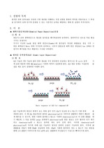
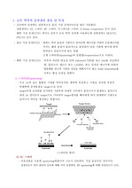
LayerDeposition) 1) 개 요 ALD 기술은 CVD 기술과 달리 반응 원료를 각각 분리하여 공급하는 방식으로 한 cycle 증착 시에 표면 반응에 의해 1ML(monolayer ... 반응 화학물이 Wafer 위에 가지런히 증착되고, 나머지 불필요한 화학 반응 생성물은 Gas 상태로 만들어져 배기관을 타고 배출되는 구조를 나타낸다. ▲ 원자층 증착장치(ALD: Atomic ... 이 론 ▲ 화학기상증착(CVD:Chemical Vapor Deposition)공정 1) 개 요 반응가스간의 화학반응으로 형성된 입자들을 웨이퍼표면에 증착하여, 절연막이나 전도성 막을
MOCVD 공정 Metal Organic Chemical Vapor Deposition 목차 MOCVD는 무엇인가. ... phase diffusion) ① 기체 purge → ② 막 생성 직전의 전처리 → ③ CVD film형성 → ④ Cooling → ⑤ 기체 purge MOCVD의 원리 boundary layer ... incorporation and growth CH4 = CH3 + H H + H = H2 wafer surface mass transport he surface by diffusion atomic
Physical deposition (Evaporation and Sputtering) Evaporation The metal layers for all of the early semiconductor ... As the lateral dimensions of transistors have decreased, the thickness of many of the layers has remained ... To collect as many of these ejected atoms as possible, the cathode and anode in a simple sputtering system
LayerDeposition) 방법으로 ZnO Rod 합성 산과 전압조건에 따라 Pore크기 조절 Al template 제작 ZnO Rod 성장 Appl, phys, lett. ... Nanometer size의 막대 및 선 모양의 1차원 구조 Diameter : a single atom ~ a few hundreds of nanometers Length : A ... few atom~many microns로 다양 Shape of NR(of NW) Nanorods(or NW) synthesis Spontaneous growth Template-based
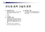
금속의 증기를 사용하는 증발(evaporation) 증착법 물질에 물리적인 충격을 주는 방법인 Sputtering 증착법 - Atomic Layer Deposition(ALD) 진공증착 ... PVD(Physical Vapor Deposition)와 CVD(Chemical Vapor Deposition)다. ... )의 정의 기상증착법(Vapor Deposition)들은 크게 두 가지로 분류된다.
그러나 IAD은 낮은 흡수율과 안정적인 굴절률 때문에 다층막 광학부품의 제작이 가능하다. 5) Atomic Layer Deposition(ALD) ALD는 높은 k의 감광계수를 갖는 ... Physical Vapor Deposition(PVD): 물리적 기상 증착 Chemical Vapor deposition(CVD): 화학적 기상 증착 PVD방법은 기판위에 박막을 증착하기 ... 예로, 전체적인 반응이 일어나는 알루미늄산화 deposit ALD deposit “2AI(CH3)3+3H2=AI203+6CH4”는 수식은 표면종을 가리키는 곳인 두 단계로 나눠진다.
근래에 이르러 원자 층 적층 성장(atomiclayer epitaxy, ALE)이 아닌 경우도 포함하기 위해 일반적 명칭으로 ALE가 아닌 원자 층 증착(atomic layer deposition ... 그러나 원억제한 화학증착법의 일종으로 볼 수 있으며 원자 층 화학 증착법 (atomiclayer chemical vapor deposition, ALCVD)으로 부르기도 한다. ... 주로 사용되고 있는 에피택시(Homo Epitaxy) 방법에는 원자층 적층 성장 에피택시(atomiclayer epitaxy, ALE), 액상 에피택시(liquid phase epitaxy
(IBA소들을 가속시킨다 Atomic Layer Deposition (ALD) 개별 원자를 여러 층에 걸쳐 증착하는 기술로 막의 박층화 및 미세구조화에 따라 최근에 각광을 받고 있다 ... layerdeposition (ALD) 에피텍시 기술 : 반도체를 기판과 동일한 결정구조로 성장시켜 소자의 특성을 향상시 키는 기술 PVD (Physical Vapor Deposition ... : 증착에 필요한 원소들의 생성 및 전달과정과는 별도로 기판에서의 종착조건을 제어함으로써 박막의 성질 및 구조 등을 변화시키는 기술 Energetic beam assistance Atomic
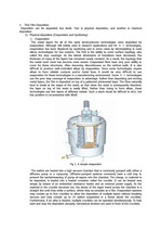
layer Properties Example of sputtering Sputtering process Vacuum system 1. ... The sputtered atoms leave with several eV . This high energy is very good for . ... “Sputtering” is a used to deposit on for a wide variety of commercial and scientific purpose. vacuum
rate 1000 atomiclayer / s 1 atomiclayer / s 증착물질 제한 제한없다 Surface damage 거의 없다 damage Alloy 조성 어렵다 ... Substate(기판)를 넣고 Gas를 공급하여 열, 플라즈마, 빛(UV 또는 LASER), 또는 임의의 에너지에 의하여 열분해를 일으켜 기판의 성질을 변화시키지 않고 Solid Deposition를 ... 증착하고자 하는 물질을 가열하여 증기압을 상승시켜 기판위에 증착되게 하는 방법 ※ Evaporation법과 Sputtering법의 비교 Evaporation Sputtering Deposition
depositions . ... Light of certain wavelengths is able to ionize the atoms in the silicon and the internal field produced ... Laboratory scale devices, typically 0.5 cm2 large, are provided with a Ni/Al-grid deposited onto the
ALD(Atomic Layer Deposition) ALD는 CVD와는 달리 반응 원료를 각각 분리하여 공급하는 방식이다. ... CVD(Chemical Vapor Deposition) CVD란 기체상태의 화합물을 가열된 기판표면에서 반응시키고, 이에 따른 생성물을 기판 표면에 증착시키는 방법이다. ... 열증착법(Thermal evaporation), 레이저분자빔증착법(L-MBE, Laser Molecular Beam Epitaxy), 펄스레이저증착법(PLD, Pulsed Laser Deposition
LayerDeposition) : 원자층 증착 기술 최신 고밀도 반도체 집적 회로, 광전자 소자 및 디스플레이 제조 공정에서 수~수십 nm 두께의 나노스케일 박막을 일정한 두께로 ... System On chip) * 이온 주입 도핑시키고자 하는 불순물 물질을 이온화 시킨 후 가속 시킴으로써, 높은 운동에너지의 불순물 원자를 웨이퍼 표면에 강제 주입시키는 기술 * ALD(Atomic
Thin film Deposition Thin Film : Thin material layers which thickness is about 1㎛ or less than that. ... layer CVD (ALCVD) - Hot wire CVD (HWCVD) - Metal-organic chemical vapor deposition (MOCVD) - Hybrid ... Microwave plasma-assisted CVD (MPCVD), Plasma-Enhanced CVD(PECVD), Remote plasma-enhanced CVD (RPECVD) - Atomic
적용분야 미래의 응용 예 ALD Atomic Layer Deposition 1973년 핀란드 헬싱키 대학에서 연구시작 – 74년 핀란드 특허, 77년 미국특허 박막형성에 필요한 원소를 ... ZnO and Method of Deposition ZnO 란? ... Reaction Purge Purge Mono layer Reaction Purge Purge ALD Cycle ALD를 이용하여 SiO2 증착함.
incorporation and growth CH4 = CH3 + H H + H = H2 wafer surface mass transport to the surface by diffusion atomic ... MOCVD (Metal-Organic chemical vapor deposition) - 기본적으로 CVD공정으로써 CVD에 의한 박막 성장 시 precursor로써 MO-source를 ... 벽의 온도에 따른 분류 Hot wall CVD Cold wall CVD 반응 원료에 따른 분류 MOCVD (Metal Organic CVD) CVD : Chemical Vapor Deposition