NiO catalysts/Al2O3/FeCrAl alloy foam for hydrogen production was prepared using atomic layer deposition ... the role of a passivation layer. ... FeCrAl alloy foam and Al2O3 inter-layer were used as catalyst supports.
Then a layer of the same physical properties as the vacuum deposition will be made, but it is not. ... Ar and ionized particles described above collide with each other at high speed on the depositionlayer ... layer penetrates into the inside of the substrate, and the adhesion is very high.
thicknesses are in the range of one or a few atomiclayers.affect the motion of electrons leads to " ... technology ↑ → semiconductor industry ↑MBE (molecular beam epitaxy)MOCVD (metal-organic chemical vapour deposition ... Introduction- Semiconductor quantum well and superlattice structures are ultrafine layered media layer
ALD 장비 특성 √ ALD는 ALCVD(AtomicLayer Chemical Vapor Deposition)의 약자로 원자층 화학증착법으로 해석할 수 있다. ... ALD(AtomicLayer Deposirion ; 원자층 증착) 1. ... Cu seed layer Cu Dielectric , SiNx
In the above state, a deposition region is formed in the semiconductor . This is important. ... Then the resulting electron and hole are moved by the field and collide with the atom to create another ... a p+-n or a p-n+ junction, it is common to terminate the lightly doped region with a heavily doped layer
ALD (원자층 증착법, Atomic layer Deposition) 원자층 증착법이란 자기 제한 반응과 표면 반응을 메커니즘으로 하는 화학 기상 증착기술이다. ... 진공 중에서 증착을 하거나 이온을 이용하는 방법이 PVD(Physical Vapor Deposition)이다. ... 아래 오른쪽 그림은 PLD(Pulsed Laser Deposition)이며, 이것은 증발시키는 것이 아니라 laser beam을 쏘아 플라즈마를 발생시켜 증착하는 것이다.
layerdeposition)에 의해서 만드는 박막 - 나노입자들의 자기결합에 의해서 만들어지는 광결정(photoni다. ... layerdeposition)등을 포함하는 증기상 입자 성장 - 나노입자의 합성을 위한 콜로이드방법과 단층 자기결합(monolayer self-assembly) 기술등이 포함되는 ... 실험 이론 ④ 나노물질 또는 나노 구조를 만들기 위한 다양한 기술 * 합성기술을 성장매체에 따라 분류 - 나노입자 합성에 이용되는 레이저 열분해나 박막증착에 이용되는 원자측 증착(atomic
마지막으로 기존의 PVD와 CVD의 한계점을 극복하기 위해 새로이 주목받고 있는 ALD(atomic layer deposition)가 있다. ... CVD PECVD 먼저 CVD(chemical vapor deposition), 화학 기상 증착법이 있다. ... Sputtering PVD(ion beam) PVD(physics vapor deposition)는 증착하고자 하는 박막의 재료를 진공 중에서 증발 또는 스퍼터링과 같이 물리적인 반응을
Atomic Layer Deposition 3. ... LayerDeposition Step of depositing uniform layer by using an inert gas Uniformity is better than that ... Remove impurities BOE : Remove the natural oxide d Fume hood Fume hood 출처 :commons.wikimedia.org ALD Atomic
스웨덴 Uppsala Univ.는 ALD(atomic layer deposition)-성장된 Zn(O,S)와 (Zn,Mg)O에서 각각 18.5%와 18.1%의 태양전지를 보고하였다. ... 독일의 ZSW에서는 단일접합 CIGS 박막태양전지(CBD-CdS 버퍼; chemical bath deposition)를 유리 기판 위에서 개발하여 다단계 동시증발법에 의한 소면적에서
LayerDeposition W, ALD W)'을 통해 삼성전자는 셀 영역의 높이가 20% 낮아짐에 따라 증가하는 간섭 현상을 줄여 동작 오류를 방지하고, 동작 인식 범위를 넓혀 ... 1.4기가비트(Gb)에 이르고, 동작전압은 33%나 낮춰(1.8V→1.2V) 4세대와 동일수준의 소비전력량으로도 최고성능을 구현한다. ② '고속 . ③ '텅스텐 원자층박막 공정 기술(Atomic
layerdeposition CVD 의 한계 극복 ! ... Step Coverage Good Uniformity Good Crystallinity Impurity, Defect Free Film Low temperature process Atomic ... KIST Definition (1991) - Thin Film : 기판층 (substrate layer) 에 형성된 수 m 이하의 두께를 갖는 것으로 독립적인 기능을 보유한 막
Here, we studied the effect of heat treatment of the thin Cu seed layer on the deposition rate of electroplated ... size, morphology, electrical properties, and electrodeposition thickness by X-ray diffraction (XRD), atomic ... Moreover, the deposition rate of electroplated Cu was improved about 148% by heat treatment of the Cu
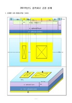
SiN over wafer ∙ Deposit photoresist over SiN layer SiN : 1200Å LPCVD 공정이용 Form Active Region c SiN ... PMOS Fabrication Process Gate Oxide 200Å Poly Gate 3000Å N-well Dose 1.0 x 10 16 atom/Cm -2 Source Drain ... substrate n-well Screen Oxide(300Å) 를 통해서 인을 주입하는 과정 900 ℃ 50min N-well E=150keV, Dose : 1.0 x 10 16 atom
Epitaxial graphene on Ir (111) crystal → atomic hydrogen was deposited onto the graphene layer at room ... hydrogen was deposited onto the graphene layer at room temperature by means of 1600 K hot H-atom beam ... (Hydrogen atom on Graphene) Atomic Hydrogen Adsorbate Structure on Graphene ♦ STM images of hydrogen
Furthermore, the overall atomic concentration of the oxygen in the buffer layer decreased because deoxidation ... In this study, chemical bath deposited (CBD) indium sulfide buffer layers were investigated as a possible ... to indium oxide and indium sulfide from the as-deposited indium hydroxide and sulfate states.