and a-Si:H layer. ... Atomic concentrations and relative oxidation states of Si, O, and Zn were analyzed by AES method. ... One sample was deposited by ZnO:Al at low working pressure.
Atomic Layer Deposition Technology ALD (Atomic layer Deposition) previously known by the name ALE (Atomic ... Atomic Layer Deposition Technology Mechanism of ALD ALD Process Features ALD vs. ... Conventional CVD Application of Atomic Layer Deposition Transistor Gate Dielectrics MEMS Opto-Electronics
Ni, mean particle size and specific surface area of the composite powders were investigated by Atomic ... Ni-diamond composite powders with nickel layer of round-top type on the surface of synthetic diamond ... these relatively thick layers with nodule-type on the surface of diamond by a lateral growth mechanism
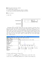
본 논문은 메탈 이중층 전극을 이용한 유기 박막 트랜지스터를 제작하여 Au나 Ag 금속만으로 제작한 일반적인 유기 박막 트랜지스터와의 전기적 특성을 비교하였다. 전기적 특성에서 게이트 절연층은 높은 K 값을 갖는 Al2O3를 사용하였고, 유기 반도체층은 펜타센을 사용하..
and to the active participation of incorporated Mg atoms. ... Mg-doped and In-Mg co-doped p-type GaN epilayers were grown in a low-pressure metal organic chemical vapor deposition ... For the In-doped p-GaN layer, the PL intensity increases significantly and the peak position shifts to
The results shed light on the atomic layer deposition process of alternate gate dielectric materials, ... Si atom, and the H atom of the water molecule favored the up-buckled Si atom. ... and between the positively charged H of the water and the negatively charged up-buckled Si atom.
When depositing AZO thin film on a-Si layer, oxygen atoms are diffused from the AZO thin film towards ... For the Zn layer, the deposition was conducted at 5 nm, 7 nm and 10 nm using the rf-magnetron sputtering ... the a-Si layer.
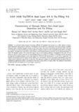
* Fig. 6 C:Al atomic ratios in a HAOPs layer with 18 g Al/m2 (a) at the top and the bottom of the layer ... NOM removal by pre-deposited HAOPs with varying surface loadings. 3.1 Removal of DOC and UV254 실험 종료 ... 막표면에 흡착제를 미리 침착시키는 것은 등가의 흡착제를 원수에 첨가하는 것보다 막오염을 저감 Study of hybrid adsorbent/membrane processes Pre-deposition
In this paper, we present a Raman spectroscopic investigation of the effects of UV light on single layer ... The UV-induced reaction was also successfully applied to chemical vapor deposition-grown graphene. ... The UV emission from a low pressure Hg lamp photolyzes O2 molecules into O atoms, which are known to
methods: 1) an Ag/AgCl reference electrode, 2) a platinum plate as a counter electrode, and 3) a seed layer ... four-point probe and the material properties were investigated by using XRD(X-ray Diffraction), an AFM(Atomic ... The electrolyte effects of the electroplating solution in Cu films grown by ElectroPlating Deposition
LayerDeposition) ★각 반응 물질들을 개별적으로 분리해 반응기에 공급하여 기판표면에 반응물질이 표면포화 반응에 의해 화학적 흡착과 탈착을 하고, 이를 이용하여 박막을 ... Enhanced CVD) Photon Energy : PCVD Laser Energy : Laser CVD 기판 가열 방법에 따라 Hot Wall Cold Wall ALD 원리 ALD (Atomic ... 화학반응을 통하여 as를 공급 Energy부에서 공급된 Energy(열 ,플라즈마 , 빛 등) 에 의하여 분해, 반응시켜 기판에 박막을 형성 CVD Mechanism Boundary Layer
A new cost-effective atomic layer deposition (ALD) technique, known as Proximity-Scan ALD (PS-ALD) was ... Under an optimized deposition condition, the deposition rates of Al2O3 and HfO2 were 1.3 Å/cycle and ... developed and its benefits were demonstrated by depositing Al2O3 and HfO2 thin films using TMA and TEMAHf
Field emission scanning electron microscopy and atomic force microscopy were used to characterize the ... localized surface plasmon resonance (LSPR) by inducing Au thin films with thickness of 0.0 to 5.0 nm, deposited ... microstructure of the blocking layer (BL) of the Au thin films.
copper composite powders were prepared by electroless plating method by controlling the activation and deposition ... It is noted that completely cleansing the copper oxide layers and protecting the copper particles surface ... the product were verified by using a scanning electron microscopy (SEM), X-ray diffraction (XRD) and atomic
In this paper, we present a Raman spectroscopic investigation of the effects of UV light on single layer ... The UV-induced reaction was also successfully applied to chemical vapor deposition-grown graphene. ... The UV-induced reaction was also successfully applied to chemical vapor deposition-grown graphene.