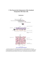
On one of these electrodes, a few micron-thick layer of TiO2 is deposited using a colloidal preparation ... To obtain supporting evidence, an electrode is prepared with a 60 nm layer of chemical vapor deposited ... To avoid any contribution from the exposed substrate, a thin layer of insolating polymer was deposited
Silicon 열산화공정 고온(800~1200도)에서 산소나 수증기를 silicon wafer표면에 뿌려 산화막을 형성시키는 공정 2 Ways to Add a Silicon Dioxide Layer ... A plasma can be produced from a gas if enough energy is added to cause the electrically neutral atoms ... of the gas to split into positively and negatively charged atoms and electrons. + + + + + + + + + +
AtomicLayer CVD (ALCVD) - A CVD process in which two complementary precursors (eg. ... Metal-Organic CVD (MOCVD) Plasma Enhanced CVD (PECVD) Rapid Thermal CVD (RTCVD) AtomicLayer CVD (ALCVD ... depositing thin films of various materials.
LayerDeposition) Carbon impurity Low temperature process Step coverage comparative good MOCVD (Metal ... Device complexity Low temperature process Step coverage good Composition and thickness control good ALD (Atomic ... ) Step coverage bad Low temperature deposition possible Impurities less PVD (Physical Vapor Deposition
Inroganic-Organic Hybrid Circuits: Nanocell Devices Assembly Langmuir-Blodgett Technique Setup for Langmuir-Blogett Deposition ... relay transistor Devices - Upon charging a gate, a mobile switching atom move into a line of atomic ... wire. - A switching atom is placed between two molecular or atomic wires and controlled by two 'gate'
Finally, an Ag layer was deposited as a protecting layer 장치제조법 가) 글래스에 ITO를 코팅하고 그 위에 PEDOT:PSS층을 스핀코팅 ... LiF (5 nm) and Ca (10 nm) were deposited as the cathode 5. ... Polymers was spin coated on the PEDOT layer as an emitting layer (70 nm) 4.
◇나노 반도체 시대 선두주자 ALD= CVD공정에서 진화된 기술인 원자층증착(ALD, Atomic Layer Deposition)공정은 말 그대로 원자 두께의 극도로 얇은 박막을 생성해 ... PVD (Physical Vapor Deposition) PVD에 해당하는 증착법에는 스퍼터링 (Sputtering), 전자빔증착법 (E-beam evaporation), 열증착법 ... ◇반도체 증착공정의 꽃 `CVD'= 반도체 제조과정의 77%를 차지하는 전공정, 이 가운데 화학증착(CVD, Chemical Vapor Deposition)공정은 13% 비율을 차지해
진공 플라즈마 시스템을 이용하는 응용분야로는 일반 반도체 공정에서 사용되는 건식 식각 공정, 증착 공정, 에싱(ashing) 공정, ALD(Atomic Layer Deposition ... 나노기술 (Nano Technology) 및 바이오 기술 (Bio Technology)분야 - ALD(Atomic Layer Deposition) 성장 기술 - 탄소나노튜브 성장기술
On a local, atomic scale, thickness variations of 2-3Å are found which are a direct result of atomic ... photoresist Etch Hard baking Develop photoresist Exposure Align masks Soft baking Coat with photoresist Deposit ... barrier layer Photolithography process(continue) Photolithography process(continue) ◈ primary flat이
LayerDeposition) 성장 기술 -탄소나노튜브 성장기술 -의료용 멸균 기술 ● 차세대 플라즈마 정의 위에서 설명된 플라즈마 발생 기술 이외에 신개념 저온 플라즈마 발생 ... 박막 증착 장비기술 -반도체 PR ashing 장비 기술 Display 기술 -디스플레이 평판 식각장비 기술 -디스플레이 평판 박막증착 장비 기술 Nano 및 Bio 기술 -ALD(Atomic
LayerDeposition) 성장 기술 -탄소나노튜브 성장기술 -의료용 멸균 기술 ● 차세대 플라즈마 정의 위에서 설명된 플라즈마 발생 기술 이외에 신개념 저온 플라즈마 발생 ... 박막 증착 장비기술 -반도체 PR ashing 장비 기술 Display 기술 -디스플레이 평판 식각장비 기술 -디스플레이 평판 박막증착 장비 기술 Nano 및 Bio 기술 -ALD(Atomic ... 전기 소자의 특성을 만들어 준다. ⓛ 화학 기상 증착 (Chemical Vapor Deposition) : 가스의 화학반응으로 형성된 입자들을 웨이퍼 표면에 수증기 형태로 쏘아(증착
) 와 ALD(Atomic Layer Deposition)같은 상온 보호막 증착기술, ink-jet imprint와 nano-imprint와 같은 새로운 lithography 공정기술 ... 개발이 필요하고 O2 Plasma 나노 dot 제조공정 및 multi-chamber 증착공정설비 등의, 새로운 집적화 공정기술, HNB(High Density Neutral Beam Deposition
2.16 Annealing of silicon crystal - 온도에 따른 annealing 결과 - ① 450℃ : 부분적 활성화, 부분적 손상 회복 ② 600℃ : epi-layer의 ... 상태에서의 확산 계수를 의미 하며 다른 물질이나 에너지를 받아 고체의 표면에 입사할 때 일어나는 현상의 하나이고 입사 이온에 따라 고체 표면의 sputtering, ion beam deposition ... Table 1.1 Solid solubility limits in silicon at 1100℃ Dopant Solubility limit (atoms/cm3) Arsenic (As
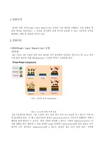
1.실험목적 원자층 단위 증착(Atomic Layer Deposition) 공정의 기본 원리를 이해하고 직접 실험을 통하여 박막을 만들어보고 그 특성을 분석하여 실제 연구에 응용할 ... 수 있는 기본적인 능력을 배양하는 데에 본 실험의 목적이 있다. 2.실험이론 1)ALD(Atomic Layer Deposition) 공정 가)특성 ALD 기술은 CVD 기술과 달리
Layer Chemical Vapor Deposition) 아래 그림(a)는 ALCVD반응기의 구성도를 간단히 나타낸 것이다. ... plasma-enhanced CVD, photochemical CVD , laser-induced CVD, electron-beam assisted CVD로 분류될 수 있다. 3.2 ALCVD(Atomic ... 박막형성 기술의 대표적 방법으로 CVD(Chemical Vapour Deposition), PVD(Physical Vapour Deposition)법 이 있으며 CVD법에 의한 박막
분자빔 에피택시 (MBE) 원자증 증착 (ALD) Atomic Layer Deposition ALD는 화학적 증착으로 반응기체를 동시 삽입하는 CVD와 다르게 반응기체를 번갈아서 넣어서 ... 분자빔 에피택시 (MBE) 화학 기상 증착 (CVD) Chemical Vapor Deposition 원료를 Gas 로 공급하여, 기상 또는 기판표면에 있어서의 화학반응에 의하여 박막을
high-energy electron diffraction (RHEED) Microstructure failure analysis Electron-beam-induced metal deposition ... Enhancement Technology Antireflective Coating (ARC)-Thin Film Interference Effect When using single-layer ... limits resolution to no better than the resist thickness Using ever thinner resist layers further improw