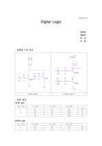
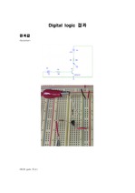
결과보고서 Digital Logic 실험일 : 제출일 : 학 번 : 이 름 : - 실험에 쓰인 회로 [NOR gate] [NAND gate] - 실험 결과 1)NOR gate V _ ... V] V _{O} [V] 5 0 0 5 H 0 5 5 H 5 0 5 H 5 5 0.2 L [NOR Gate] [NAND Gate] - 실험결론 및 토의 이번 실험은 Digital Logic의
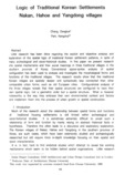
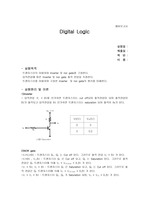
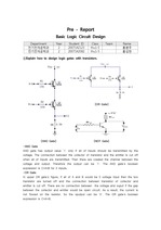
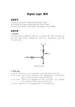
예비보고서 Digital Logic 실험일 : 제출일 : 학 번 : 이 름 : - 실험목적 트랜지스터의 이용하여 inverter 및 nor gate를 구성한다. ... 5 0.2 5 5 0.2 -실험 방법 (1)Inverter를 그림의 회로와 같이 연결 한 후 V1의 값을 0V와 5V를 인가한 후 출력 전압을 측정 한다. (2)NOR gate logic을
.2. Why even offer the Complete System? As Kuta and Lambrecht thought about their problems, they realized that a kind of system could do much more, co..
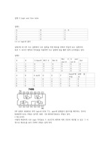
실험 2 Logic and time table 실험1. A B A . ... (그림 2)이다 이렇게 복잡하게 나온 logic 진리표도 드 모르간의 법칙에 의해 간단히 계산할 수 있고 그 이점으로 회로도를 보다 간편히 꾸밀수 있게 된다 3. ... B 1 1 1 1 0 1 0 1 1 0 0 0 1.2 or logic과 같다 실험1에 10-1번 사고 실험에서 나온 질문을 직접 회로를 꾸며서 만들어 보는 실험이다 또한 드 모르간
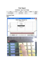
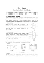
Final Report Combination Logic Circuit Design 학과 학년 학번 분반 실험조 성명 전기전자공학과 2 2007142082 thu1-5 홍성현 전기전자공학과 ... So in order not to using the Logic gates, we should use a 32×1 multiplexer because the 32×1 mux can permit
current-mode logic or current-switch emitter-follower logic. ... The equivalent of emitter-coupled logic made out of FETs is called source-coupled FET logic. ... transistor logic because both the logic gating function and the amplifying function are performed by
Digital logic 예비 실험목적 ① 트랜지스터를 이용하여 Inverter 및 NOR gate를 구성한다. ② 입력전압에 따른 Inverter 및 NOR gate 출력 전압을 ... NOR gate ① 그림2와 같이 NOR gate logic 회로를 연결한다. ② V1=V2=0V으로 전압을 인가하고 출력 전압을 측정한다. ③ V1=5V, V2=0V로 전압을 인가하고
Pre - Report Combination Logic Circuit Design Department Year Student ID Class Team Name 전기전자공학과 2 2007142123 ... The 2x1 multiplexer is data selective logic circuit because it outputs one input selected from two inputs ... Decoder> -Decoder Decoder can take the form of a multiple-input, multiple-output logic
간선도로 제어는 간선도로를 이용하는 교통류를 연속진행시키기 위한 목적으로 행한다. 간선도로의 한 교차로에서 방출된 차량군이 그다음 교차로의 녹색신호 시작 순간에 도착하여적색신호 이전에 통과를 완료하게 하되 차량군이 분산되지 않도록 인접 교차로의 신호시간을조절하여야 한다..
전자회로실험2(결과보고서) 실험 : MOSFET Digital Logic Gate 1. ... 0.23mV 5 0 26.33mV 2.59mV 0.23mV 5 5 26.31mV 2.59mV 0.23mV 5V 0V VA VB Vout 이번 실험은 MOSFET을 이용한 Digital Logic
전자회로실험2(예비보고서) 실험 : MOSFET Digital Logic Gate 1. 실험 목적 디지털 로직 게이트를 기초로 하여 MOSFET의 동작을 이해한다. 2. ... 이 무시 할 수 없는 기생저항 성분으로 인하여 이론값과의 차이가 발생하였지만, 이번 실험 목표인 Digital Logic Gate로써의 High, Low 구분 역할 수행에는 크게 문제되지
Post-Lab Report Lab#04 Combinational Logic Design 1 @ Arithmetic Logic and Comparator 담당 교수 강 상 혁 담당 ... Methods 1) Half Adder Logic design 가) 프로젝트를 생성한다. ... Full Subtractor Logic design Schematic Ucf code Ful하였다. 그 결과는 아래와 같다.
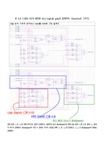
Methods 1) 3:8 Decoder Logic design 가) 프로젝트를 생성한다. ... 바) 프로그래밍을 완료 한 후 장비에서의 동작을 확인한다. 2) 2:1 Mux Logic design 가) 프로젝트를 생성한다. ... Purpose of this lab Verilog HDL을 통하여 Combinational Logic Circuit을 설계한다. 나.
The purpose of the research is to discuss the product safety procedures for the food industry The producer and supplier of the products should satisf..
Purpose of this lab Sequential Logic Circuit의 작동원리를 이해하고 Verilog HDL을 통하여 Sequential Logic Circuit을 설계한다 ... Pre-Lab Report Lab#07 Sequential Logic Design2 @ FSM and Clocked_Counter 담당 교수 강 상 혁 담당 조교 박 재 민 실 험
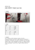
MOSFET Digital Logic Gate 1. 실험회로 NAND게이트 NOR게이트 2. ... 먼저 BJT Digital Logic을 잠깐보면 다음과 같다. MOSFET 로직 게이트의 장점은 높은 Input Impedance를 가짐으로써 전력소모를 줄인다 는 점이다.