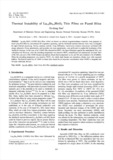
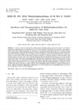
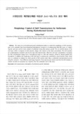
Preparation procedure of DSSC FTO (F-doped SnO 2 ) film Coating with TiO 2 paste Anneal at 450-500 o ... DSSCs 제작을 통한 원리와 구조의 이해 웨이퍼 구조 결정질 실리콘 다결정질 실리콘 박막 구조 CIGS 태양전지 Si 태양전지 CdTe 태양전지 GaAs 태양전지 광전기화학구조 염료감응형 ... µ m) (1-2.5 µ m) (0.5-1 µ m) (0.2-0.5 µ m) (0.06-0.2 µ m) (2-8 µ m) CIGS solar cell CdTe solar cell Si
deposited directly onto SiO2/Si substrates. ... deposited on self-assembled Au nanodots (SnO2/Au) that were formed on SiO2/Si substrates. ... the effect of the fabric of the surface microstructure on the CO gas sensing properties of SnO2 thin films
Process Using indums , connect evaporated Al to Al varn Connect edge of wafer to Si Measure the Capacitor ... So, from the Calculation of oxide film thickness formula, is constant. ... Introduction ZnO TFT TFT is a type of Field Effect Transistor which is form of Thin Film.
Si-DLC films were deposited by radio frequency plasma enhanced chemical vapor deposition (RF-PECVD) process ... In this study, the deposition of DLC films was carried out in vacuum with a chamber pressure of 10-5 ... as synthesized DLC films were analyzed by wear test in the presence of dry air, water and lubricant
of each of the different DLC deposition conditions, the deposition conditions of DLC + F and DLC + Si ... Also, DLC films coated on paper, polymer, and metal substrates have been extensively used. ... Diamond-like carbon (DLC) films have been widely used in many industrial applications because of their
일반적으로 TFT(thin film transistor)의 유전체막으로 실리콘 질화막(Si3N4)이나 실리콘 산화막(SiO2)을 200-300˚C의 온도에서 증착을 하게 되는데 본 ... 연구에서는 비정질 실리콘과 유전체막 사이의 계면 특성 특히 계면의 거칠기를 향상시키기 위해서 기존의 증착법이 아니라 비정질 실리콘(a-Si:H)과 산소 ECR 플라즈마의 반응에 의한
on Si substrates by vapor self assembly monolayer (VSAM) method. ... Contact angle, surface energy, film thickness, friction force, and roughness were considered for finding ... An MPTMS (3-mercaptopropyltrimethoxysilane) monolayer as an adhesion layer for Au/Pd thin films was deposited
Patterning and treatment of Sio2 thin films 나는 자랑스런 인하인으로, 스스로의 힘으로 정직하게 레포트를 작성하였습니다.” + 이름 + 서명 서론 ... (예를 들어, 실험 재료 중 한 가지는 pattern이 완료된 SiO2 wafer가 있어요) 실리콘 웨이퍼: 반도체의 기반이 되는 물질이며 순수 Si로 이루어져 있다. etching을
instability of LSMO on fused silica should be an important consideration when LSMO is integrated into Si-based ... La0.6Sr0.4MnO3 (LSMO) thin films, which are known as colossal magnetoresistance materials, were prepared ... on fused silica thin films by conventional RF magnetron sputtering, and the interfacial reactions between
Surface Wafer 산화 P-type Si Wafer 반도체 제작 공정 1-2 실리콘 산화의 방식 건식 산화 : 얇은 산화막 (Thin Film) 을 형성 시 선택 ( 최대 ... 0.9 ㎛ ) – L ow Ecth Rate 습식 산화 : 두꺼운 산화막 (Thick Film) 형성 시 선택 ( 최대 6.5 ㎛ ) – High Ecth Rate ※ 같은 Oxidation ... P-type Si Wafer Metal SiO ₂ SiO ₂ N-type Metal Polymer BOE P-type Si Wafer Metal SiO ₂ SiO ₂ Metal Polymer
We fabricated thermally evaporated 30 nm-Ni/(20 nm or 60 nm)a-Si:H/Si films to investigate the energy-saving ... confirmed that the nickel silicide had more than 50 nm-thick columnar-shaped structures with a Ni31Si12 ... temperatures below 450˚C, we confirmed columnar-shaped structures with thicknesses of 20~30 nm that had δ-Ni2Si
an effective medium theory with Bruggeman geometry consisting of a random mixture between SiO2 and Si3N4 ... and explored the effectiveness of the silicon in fine tuning the refractive index of the composite film ... The atomic fraction of nitrogen in SiOxNy films was controlled by varying the relative flow ratio of
of the film. ... Solid-state NMR is utilized to investigate the insolublesamples and the chemical shift of 29Si. ... SiOC(-H) thin films containing alkylgroup are generally prepared by PECVD method usingtrimethoxysilane
)를 Sliced Si wafer 조각에 spin-coat 시킨다. ... AFM 사용하여 PS-b-P4VP inverse micelle film과 reconstructed PS-b-P4VP film의 morphologies를 관찰한다. ... Au NP arrays deposited on reconstructed BCP films 위에서 만들고 남은 PS-b-P4VP coated slice를 하나는 EtOH에, 나머지 두
on an all-solution-processed hydrothermal method to control the morphology of ZnO nanostructures on Si ... substrates from three-dimensional hemispherical structures to two-dimensional thin film layers, by controlling ... layer concentration is increased, the ZnO nanostructures change from a hemispherical shape to a thin film
떨어져 반응성이 강한 radical이 되기 때문에 QUOTE 의 반응이 일어나 Si을 etching합니다. ... 그 중 film deposition에 대한 부분입니다. ... Film etching에 사용되는 plasma Plasma를 이용한 film etching은 물리적 방법과 화학적 방법, 그리고 물리화학적 방법으로 나눌 수 있습니다.