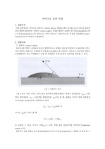
실험변수 설정 1) Thickness of film - 10nm, 20nm, 30nm (실험변수) 2) Type of metals - Al (고정) 2.2. ... 제공하기 위해 다섯 번째 공정에 해당하는 Si Wafer 위에 증착된 Ni과 Si의 Annealing을 통하여 Silicide(Ni-Si 합금)을 만드는 과정을 실시하고 Four-point-probe를 ... Wafer Cleaning Process 1) (100)방향성을 지닌 p-type Si wafer를 준비한다. 2) BOE용액에 Si wafer를 담가 30분간 cleaning 과정을
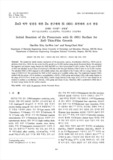
Annealing temperaturesand times affected the formation of Si QDs in the SRO film. ... Si quantum dots with a super lattice structure (Si QDSLS) were prepared by alternating deposition of ... The systematic investigation of precipitation behavior of Si QDsin SiO2 matrices is presented.
Furthermore, the thermal expansion coefficient of the aluminum nitride is similar to those of Si and ... To fabricate the AlN thin film, we used the magnetron sputtering method with N2, NH3 and Ar. ... We fabricated AlN thin films with an a-axis orientation by controlling the sputtering electric power,
process for the gap-filling of submicrometer trenches using dimethyldimethoxysilane (DMDMOS), (CH3)2Si ... We obtained low-k films with superior gap-filling properties on the trench patterns without voids or
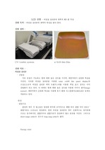
nanotube.korea.ac.kr/wp-content/uploads/2011/07/%2525EA%2525B7%2525B8%2525EB%2525A6%2525BC-11.jpg&w=510&h=238&ei=2Si7UK-hDszkmAWuj4DQAg ... 두 유리기판에 sealing film을 붙이고 코팅면이 마주보게 좌우로 살짝 어긋나도록 붙인 후, 오븐에서 125℃로 5분간 구워준다. ... 전해질을 주입한 두 개의 구멍에 sealing film과 슬라이드 글라스를 차례로 올린 후 인두로 녹여 막아준다. ? 마지막으로 silver paste를 바른다.
또한, BUMP 형성시에는 발생하지 않았던 Al 전극밑의 SiO₂ 나 Si 의 CRACK 이 BONDING 시에 발생하는 경우가 있다. ... 게다가 또, 사용하는 FILM CARRIER 나 BUMP 가 LOT 마다 변하기 때문에, 접합부도 또한 이에 따라 변한다. ... 이런 경우는, BONDING 후 에, 왕수 등으로 BUMP 나 Al 전극 등의 금속막을 제거함으로써, SiO₂, Si 표면의 CRACK 을 관찰할 수 있다.
precursors, namely, di-methylzinc (Zn(CH3)2, DMZ) and diethylzinc (Zn(C2H5)2, DEZ), for zinc oxide thin-film ... growth on a Si (001) surface using density functional theory. ... We calculated the migration and reaction energy barriers for DMZ and DEZ on a fully hydroxylized Si (
그러므로 LCD에 서 쓰던 a-Si:H보다 poly-Si으로 대체가 되어야 한다. 그 결과 LTPS 또는 oxide 반도체가 연구중 이다. ... LCD에서는 필요한 편광판, 도광판(LGP), 위상차 film, prism sheet 등의 각종 광학 film이 이제 필요가 없으며TFT는 LCD에서 단순한 switch 역할만 했지만
투사하면 X선이 산란 및 회절을 하게 되는데 이러한 회절 패턴을 분석하는 것 결정성과 회절 정도를 알아보기 위함 2) 측정조건 - 주사방법 : 2θ-θ - 시료 : 박막(thin film ... 증착을 가능하게 하기 위해 저압에서 성장 - 유 량 : Ga - 4.0 sccm NH₃- 1.8 slm ┗ 가장 적절한 비율 (논문참고) - 기 판 : Si ... 실험실의 보유량을 고려 * 조에서 설계한 조건 - 온 도 : 1040℃ - 압 력 : 100 torr - 유 량 : Ga - 2.0 sccm NH₃- 1.8 slm - 기 판 : Si
실험 장비 : UV-visible system a-Si:H thin film 실험 이론 : 비정질 실리콘 - 산업성 저온 공정이 가능하고 빛에 대한 높은 감도를 가지며, 대면적에서 ... 수식은 아래와 같다. ( T=투과도, d= film의 두께, Rij= 반사도) 이렇게 계산된 광 흡수 계수는 왼쪽 아래와 같은 그래프를 가지게 된다. ... 고 찰: a-Si에서 의 옵티컬 밴드갭이 2.6eV, p-Si의 옵티컬 밴드갭이 3.4eV 정도로 a-Si의 옵티컬 밴드갭이 더 낮게 측정되는 것을 볼 수 있는데, 이는 p-Si의
The set of Cu/Sn/Zn/Cu multi metal films was deposited on a Mo/SiO2/Si wafer using dc sputtering. ... CZTS films were prepared through a sulfurization process of the Cu/Sn/Zn/Cu metal layers at 500˚C in ... The metal film prepared by one-cycle deposition of Cu(360 nm)/Sn(400 nm)/Zn(400 nm)/Cu(440 nm) had a
그림-5에서 Si, Ti, Zr등이 입사할 때 sputtering yield가 크게 감소하는 것을 볼 수 있다. ... 000 < sputtering > →목적물 표면에 막의 형태로 부착하는 기술 세라믹이나 반도체 소재 등에 전자 회로를 만들기 위해 고진공 상태에서 고체를 증발시켜 박막 thin film ... 이나 후막 thick film 을 형성하는 경우에 사용 된다. (1) 원리 Sputtering은 chamber 내에 공급되는 gas cathode에서 발생되는 전자 사이의 충돌로부터
angle Al 79.14 Si 95.91 PDMS 68.59 nano film 59.27 3) 실험에 사용된 substrate의 표면특성을 실험결과인 contact angle, ... 접촉각(contact angle)이 90˚이하인 Si와 Al은 젖음성이 높은 친수성이라고 볼 수 있다. 또한 상대적으로 표면에너지가 높은 재료이다. ... 고찰 1) 실험에 사용된 substrate의 종류에 따른 static contact angle의 그래프를 작성하시오. substrate Average angle Al 85.02 Si
Thin film type Reference : 김성수 . ” 주울 가열을 이용한 AMOLED 패널 봉지기술 개발 ” , 홍익대학교 , p.11-14(2011) - 무기물과 유기물의 ... Backplane 구현을 위한 TFT - Si 기반 TFT : poly-Si TFT, nc -Si TFT, a-Si TFT - 유기물 반도체 기반 TFT : Organic TFT(OTFT ... 등의 단점을 보완하기 위해서 a-Si TFT, OTFT, Oxide TFT 등의 기술이 활발히 이루어 지고 있다 .
Keyword: silicon carbide, coating, film, preceramic polymer, spin coating, energy
efficiency 한국열환경공학회 ... coating on the silicon
wafer, polycarbosilane was decomposed away its organic pandents and remained Si-C
Deposition(증착), Thin Film - 물질을 쌓아올리는 과정 PVD - 물리적 증착(금속 박막 증착에 주로 쓰임), CVD - 화학적 증착 Metal interconnect ... cross talk 현상을 해결해줌 - 3D Vertical Nand : 원통형으로 쌓아올리기, 수직으로 쌓아올리기 - Nano 3D Vertical Nand : 원통의 Poly-Si를 ... 웨이퍼 - GaAs, Si를 기둥으로 성장시켜 자르고 평평하게 만드는 작업 Oxidation - SiO2를 형성하기, 불순물로부터 웨이퍼 보호 건식 산화 - 산소만을 이용 오래걸림
Sharp, Japan c-Si, Thin FilmSi 745 9 Motech, Taiwan c-Si 715 10 Kyocera, Japan c-Si 532 c-Si ... 5 Trina Solar, China c-Si 1,116 6 Q-Cells, Germany c-Si, CIGS 939 7 Gintech , Taiwan c-Si 800 8 ... Silicon solar cells are classified by using either single crystal wafer, polycrystalline wafer or thin films
Photolithography 공정은 일반사진의 film 에 해당하는 photo resist 를 도포하는 PR 도포공정 , mask 를 이용하여 선택적으로 빛을 조사하는 노광공정 , ... effect transistor) 15 스위치 소자의 역할 MOSFET Metal oxide semiconductor field effect transistor TFT Thin film ... 형태에 따른 분류 Projection lens 접목렌즈 투사형 LCD 액정셀 거울 액정셀 거울 액정셀 반사형 LCD 투과형 LCD 3 단자 AM-LCD : TFT LCD (thin film