The titanium was deposited on a SiO2/Si substrate by the DC magnetron sputtering method and was oxidized ... The titanium film originally had smooth surface morphology, but the film agglomerated to nano-size grains ... Titanium dioxide thin films were fabricated as hydrogen sensors and its sensing properties were tested
Aluminum nitride(AlN) films were grown on the C-face and on the Si-face of (0001) silicon carbide(SiC ... polarity and, first-stage growth manipulation strongly affected the growth and properties of the AlN films ... Al pre-exposure on the C-face and on the Si-face of SiC substrates prior to initiation of the AlN growth
CZTS films were directly synthesized on Mo/Si substrates by chemical bath deposition method using copper ... morphology, whereas the film sulfurized at 5% H2S yielded a very smooth and dense film morphology. ... The CZTS films sulfurized at low H2S concentrations of 0.05 % and 0.1% showed very rough and porous film
Screen Film은 quantum efficiency가 약 2%로 매우 비효율적이다. ... light로 바꾸는 특성을 이용하여 image를 얻는데 이 image의 QE는 약 25%이다. hydrogenated amorphous silicon detectors(a-Si:H ... 발전적으로, photographic plates과 photographic film을 거쳐 현재는 image plates나 flat panel detectors와 같은 digital
한국재료학회 한국재료학회지 Cho, Ho Je, Seo, Yong Jun, Kim, Geun Woo, Park, Keun Young, Heo, Si Nae, Koo, Bon Heun ... level, oxygen partial pressure, substrate temperature, and film thickness. ... The crystallinity of the films also increased with the substrate temperature.
tape 제품 생산 공정 ..PAGE:5 Si PSA 특/장점 ..PAGE:6 실리콘 점착제 사용분야 Electronics Packaging Protective Tapes/Films ... ..PAGE:12 Si tape 제조 공정 & mechanism ..PAGE:13 Si tape 제조 공정 & mechanism ..PAGE:14 Cure system에 따른 비교 ... tape 점착성 ..PAGE:16 Si PSA Test 방법 ..PAGE:17 Si PSA Test 방법 ..PAGE:18 Summary Silicone PSA 는 - 유기점착제가
pressure and showed an amorphousstructure unlike that of films on Si substrate. ... TiO2 thin films for high energy density capacitors were prepared by r.f. magnetron sputtering at room ... TiO2 films deposited at10~30mTorr showed dielectric breakdown at applied voltage of 7V.
SiO2초박막(ultrathin film)의 두께 조절 용이성, 두께 균일성, 공정 재현성 및 전기적 특성을 향상시키기 위해 실리콘을 N2O분위기에서 열산화시켰다. ... 이와 같은 전기적인 특성의 향상은 산화막 내부에서 약하게 결합하고 있는 Si-O 결합들이 Si-N결합으로의 치환과 스트레스 이완에 의하여 감소하였기 때문이다. ... 질화 현상에 의해 형성된 Si-N결합 형성은 습식 식각율과 ESCA분석으로 확인할 수 있었다.
Ge thin films were grown on a TiN(50nm)/SiO2/Si substrate by varying the growth conditions of the reactive ... Polycrystalline germanium (Ge) thin films were grown by metal organic chemical vapor deposition (MOCVD ... H2 gas helps to remove carbon from Ge film for a Ge(allyl)4 precursor but not for a GeH4 precursor.
BiFeO3 (BFO) thin films were prepared on Pt/TiO2/Si substrate by r.f. magnetron sputtering. ... BFO films showed poor P-E hysteresis loops due to high leakage current. ... (Fe+Mn)/Bi ratio of BFO thin films increases with increasing partial pressure of O2 gas.
Indium Gallium Zinc Oxide (IGZO) thin films were deposited onto 300 nm-thick oxidized Si substrates ... These results demonstrate that IGZO thin films are suitable for use as transparent thin film transistors ... The transmittances of the IGZO thin films were approximately 80%.
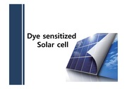
Introduction Dye-sensitized solar cell Conclusion 01 02 03 04 05 06 00 -1- I ntroduction 2 nd Gen : Thin film ... Moreover, DSSC shows higher conversion efficiency than polycrystalline Si in diffuse light or cloudy
TiO2 페이스트 소결 시 고온 (450℃)에서 분해되어 제거되면서 소결체 내부에 공극을 형성되며, 형성된 공극 사이로 염료가 흘러 들어가 흡착 된다. ② Surlyn (Film) ... 높은 발전효율/ 낮은 발전단가/ 20년 이상의 장수명/ 원료의 가격이 기존의 태양전지에 비해 저가여서 향후의 큰 시장 형성가능/ Si 태양전지에서와 같은 고가 대형 장비가 필요 없이
The electroplated Cu films were deposited on the Cu(20 nm)/Ti (20 nm)/p-type Si(100) substrate. ... density and the decrease of the electrical resistivity of the electroplated Cu film. ... The electrolyte effects of the electroplating solution in Cu films grown by ElectroPlating Deposition
With capacitance-voltage measurements of the Al/ALD-Al2O3/p-Si structure, the dielectric constant of ... Aluminum oxide (Al2O3) thin films were grown by atomic layer deposition (ALD) using a new Al metalorganic ... The ALD process showed typical self-limited film growth with precursor and reactant pulsing time at 250
Amorphous BaTi4O9 (BT4) film was deposited on Pt/Si substrate by RF magnetron sputter and their dielectric ... BT4 film. ... temperature showed the film was grown well on the substrate.
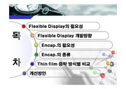
의 종류 Thin film type 장점 단점 가장 얇게 봉지 가능 다층 증착으로 공정시간 장기화 Thin film 증착 방식 Sputtering PECVD 박막증착 방식 ALD Sputtering ... Youm . 2013 Flexible Display 의 필요성 디자인의 자유화 출처 : Asus design 2010 Display mode LCD OLED TFT Array a-Si ... 내열성 약함 투명성과 제조원가적 측면에서 Flexible Display 의 궁극적인 기판 기술 ☞ 플라스틱 TFT Flexible Display 개발방향 Gate Substrate Si
The deposition process for the gap-filling of sub-micrometer trenches using DMDMOS, (CH3)2Si(OCH3)2, ... We obtained low-k films that possess superior gap-filling properties on trench patterns without voids
The structural and electrical properties of amorphous BaSm2Ti4O12 (BSmT) films on a TiN/SiO2/Si substrate ... The quality factor of the BSmT film was as high as 67 at 6 GHz. ... The temperature coefficient of capacitance of the film was low at nearly 296 ppm/˚C at 100 kHz.