OFDM System, Switchable inhibitory behavior of divalent magnesium ion in DNA hybridization-based gene ... on (In, Ga) Co-Doped ZnO Multi Deposition Thin Films Introducing Designed Bottom Layers, Hybrid Analog ... , Hybrid Precoding Based on Matrix-adaptive Method for Multiuser Large-scale Antenna Arrays, Quantitative
Lithium extraction can be achieved through two primary methods: from brine deposits and hardrock sources ... Because of this feature, it is used to store energy generated from renewable sources like solar and wind ... This process includes techniques such as precipitation, solvent extraction, or ion exchange to eliminate
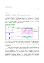
FDSOI의 경우 source와 body 사이에 유의한 potential barrier가 없기 때문에 hole은 body potential을 높이지 않고 source에서 쉽게 recombination할 ... SIMOX는 다른 SOI 기술에 비하여 etching, deposition없이 일반적인 공정들을 사용하므로 공정자체의 정확성과 투명성이 보장되는 장점을 갖고 있다. ... SOI 소자의 경우 source/drain과 substrate간의 junction이 없으므로 junction capacitance가 크게 주는 것을 알 수 있고, 아울러 소자의 크기를
ion beam injection. ... deposition (CVD) is one of the mapproximately 50% of the total wafer-processing time. ... , and reactive ion etching (RIE) which is the combination of plasma and sputter techniques.
특징을 보면 장점으로, 증착속도가 빠르고 고융점 재료의 증착이 가능하며 Multiple deposition이 가능하지만, 단점으로는 X-ray 발생과 e-beam source 위에 ... 열 source로는 고융점의 filament, baskets, boats, 그리고 용융점이 높은 재료의 evaporation에 적합한 electron beam이 있습니다. ... 열 source의 소재로는 텅스텐(m.p.:3380℃, 10-6 Torr 에서는 2410℃), 몰리브덴(m.p.:2510℃, 10-6 Torr 에서는 1820℃), 탄탈륨(m.p.:
Fig. 3(a) shows the Ion-Ioff comparison between TFET and MOSFET with different supply voltages from 0.6V ... Thus, TFET provides superior Ion/Ioff ratio of about eight orders of magnitude even at Vdd=0.2V (inset ... linear current onset in the output characteristic. where coefficients a and b are defined as where mr
이후 chamber의 source A를 제거한 후 source B를 주입하면, 기존에 형성된 film과 B가 반응하여 one layer가 coating된다. ... 이러한 sputtering 공정은 adhesion과 step coverage 우수하고, deposition rate가 일정하다는 장점이 있다. ... 다음으로는 ALD process(Atomic Layer Deposition)로, atomic scale에서 substate에 one layer씩(cycle) 반복하여 쌓는 공정이다.
PMOS Source, Drain 형성 NMOS source, drain형성과 동일하게 wafer표면에 PR을 형성하고 Photo-lithography를 이용하여 source, drain ... 이때 sputtering 방법을 사용할 수 있다. Contact을 통하여 metal과 source, drain이 연결된다. ... 산화막 위에CVD(Chemical Vapor Deposition) 로 질화막을 증착시킨다.
) 농도의 정확한 조절 및 균일성의 장점 but 격자 결함이 생김 Impantation System : 1) Generation : Ionsource Hard Mask Local ... 외부 전기장에 의해 작아진 유전체 내 전기장 세기) Capacitor = 극판 면적 & 유전율 비례, 극판 거리 반비례 -> High k 물질 필요 PN junction의 구조 : source ... Ks Atomic Layer Deposition [as aspect ratio goes high conventional CVD cannot be possible -> ALD/ALE
RTP의 필요성 예를 들어 MOS제작중일때, drain 부근에서 ion implantation 방법을 이용해서 pre deposition 후에 annealing 과정을 거치게 되는데 ... Si source SiH4 gas SiH4 gas SiH4 gas Target SEM, TEM SEM Scanning electron microscope의 이니셜이고 주사전자현미경이라는 ... wall Cold wall 공정 시간 Long time Short time 온도 변화율 Small dT/dt Large dT/dt Cycle time High low RTP의 heat source
공기가 존재한다면 공기 입자가 존재해서 source가 날라가다 충돌해서 증착될 수 있기도 하다. ... RF AC power source 부도체는 금속이 아니어서 DC에서는 Ar이 표면에 가속시킬 수 없어서 특정한 주파수로 계속 + - 로 바꿔줘여한다. ... CVD (Chemical Vapor Deposition) 화학적 물질을 증발시켜 웨이퍼 표gas를 N2가스와 함께 이동시킨다.
Based on the data, the decisions are made in stateful inspection and it is based on the sessions that ... It allows the actions to the firewall to prevent the system at the time of particular sessions carried ... is detected; The dynamic packet filtering firewall allows only a particular packet with a particular source
Electron impact ionization은 ionsource는 시료를 전자빔에 노출시키면 전자가 중성 분자와 충돌하고, 중성 분자로부터 또 다른 전자를 때려내어 시료를 이온화시킨다 ... Mass analyzer는 linearion trap을 사용하였다. 이는 quadrupole 방법의 3D version이다. Sample은 고압/저압 구간을 차례대로 통과한다. ... 하지만 sample이 유실될 수 있으며, salt에 의해 ion suppression effect가 발생하여 sample이 손상될 수 있는 단점이 있다.
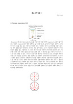
Handbook of ionsources. CRC Press. p. 222. ... : Cu Boat(source basket): tungsten boat Process current: 90A, 95A Process time: 8min Process pressure ... 이루어지므로 불균일한 증착두께가 나올 수 있다. 2) 실험 과정(최대한 상세히 서술) 이번 PVD, Thermal evaporation 실험에 대한 정보는 다음과 같다. metal source
MOSFET의 동작 영역에서 직류 전달 특성은 linear region에서 출력 전압이 입력전압과 거의 같고, saturation region에서 출력전압은 gate voltage에서 ... 다음으로 Epitaxial layer를 Si에 deposition함으로써 latch up을 감소시킬 수 있다. ... LPT(Latch up Protection Technology)회로, Transistor간 절연장벽, epitaxial wafer, Ion implant로 retrograde well