Recent Advances in Bulk Heterojunction Polymer Solar Cells -New Materials and Design Rules- 1 Contents 1 . Introduction 2. New Materials and Design Ru..
What is HEMT ?✓ HEMT : High electron mobility transistor✓ MODFET: modulation- doped FET< 중 략 >HEMT1)Buffer layer : to make Smooth surface, good to acc..
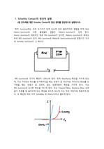
Homo-Junction의 대표적인 예로 PN-Junction이 있다면, Hetero-Junction의 예로는 바로 MS-Junction이 있다. ... 먼저 Junction에는 크게 두가지가 있게 되는데 같은 물질끼리의 접합을 하게 되는 Homo-Junction과 다른 물질들의 접합인 Hetero-Junction이 있게 된다. ... MS-Junction은 Metal과 Semiconductor을 접합시킨 것으로 Schotty-Junction이 그 예이다. MS-Junction은 두가지 특성이 나타나게 된다.
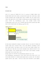
그림7에서 특히 bulk hetero junction (BHJ) 구조는 bi-layer 구조에 비해 D/A계면의 면적이 매우 커 전하 분리의 가능성이 더 큼을 알 수 있는데, 기존 ... Schematic device structures of typical organic photo-voltaic cells; (a) bi-layer structure and (b) bulk hetero-junction
In a p-n junction, current typically flows only in the forward direction. ... Additionally, the diode equation resembles the following expression for a p-n junction. 14. ... The value of the work function varies depending on the type of metal and can change when junctions are
격자부정합을 피하기 위해 hetero-junction cell을 제작하기도 합니다. 2) 2,6족 Direct transition band structure을 가지고, Hetero-junction ... 이러한 세 물질을 '물리적'으로 붙이면 hetero-junction stress가 상승하게 되므로 이들 사이사이에 Buffer layerells) Si 반도체와 화합물반도체 모두 O2를
with an active p-n+ junction. 10. why a p+-n-n+ or a p+-p-n+ junction are used? ... PN Junction is the minority carrier, and Schottky is the current flow by the mezzotint carrier. 14. ... The result is a p+-n-n+ structure with the p-n+ layer serving as the active junction, or a p+-n-n+ device
원리 반도체의 원리 LED는 P-n junction을 이용하여 만든 것으로, P-n junction을 이해하기 위해서는 일단 반도체에 대해서 알아야 한다. ... hetero) 구조로 개는 기술부족으로 백색 LED가 형광등을 대체하고 있지 않지만, 향후 기술혁신의 진보로 형광등은 물론 모든 조명을 LED로 대체할 것으로 전망된다. ... 직접 천이형의 반도체로서 발광 효율을 개선하기 위해 단일이종(single hetero) 구조의 발광층에서 하나 더 끼워 넣어 양측으로 만들어 캐리어를 가둘 수 있는 이중이종(double
=D-loop Crossing-over Two Holliday Junction Branch Migration Forms Hetero duplex Hetero duplex? ... Requirement Crossing-over가 일어나는 지역 서열 동일 dsDNA간 complementary base pairing 발생 DNA endonuclease와 ligase 효소의 작용 Hetero ... Crossing-over Two Holliday Junction Branch Migration Forms heteroduplex Resolution Result Endonuclease
Junction Band gap SKKU Light Dangling bond CdS Nano scale Dangling bond 의 감소 Surface recombination 의 ... Particle size Shape Bandgap Optical property Quantum Confinement 일반 CdS 2.5eV 3.5eV Confinement effect Hetero
Current Electron Charge Electron Diffusion Coefficient Cross section area Where ..PAGE:18 GaAs HBT (Hetero-junction ... drain current for a conventional and pseudomorphic HEMT with 0.5 um * 120 um geometry ..PAGE:17 HBT (Hetero-junction ... 구조 - BJT와 GaAs 재료의 두가지 장점을 포함 - Hetero-material devices - energy bandgap engineering device 2.
Gate → (-) voltage, Substrate → (+) voltage - In GaN area, it influence same as forward bias of p-n junction ... Source/Drain → Ohmic contact, Gate → Schottky contact: control current Formed 2DEG from AlGaN/GaN hetero ... interruption increased by different atomic size. → decreased electron mobility - Carrier mobility of hetero-structure
분야 6 조 LED: Light Emitting Diode 6 조 발광 다이오드 (LED: Light Emitting Diode) PN 접합 또는 이중이종접합구조 (double hetero ... junction) 로 이루어진 반도체 소자 LED 는 기본적으로 3mm, 5mm 정도의 크기지만 요즘은 Chip LED 시장도 많이 커지고 있으며 국내에서도 여러 모양의 형태로 개발되고
유전 (유전자간의)재조합 Crossing-over Holiday junctionHetero duplex The book says The new combination by Homologous ... Crossing-over가 일어나는 지역 sequence 동일 dsDNA간에 complementary base pairing 발생 DNA endonuclease와 ligase 효소의 작용 Hetero ... Homologous Recombination Instinct for living Diversity Needed Recombination Mutation Crossing-over Holliday junction
결국 Diode의 Threshold Voltage Vth ≈ VD 그림 1.1 (a) p-n junction under zero bias, (b) Forward bias. 2. ... Heterojunction의 단점 ① Resistance caused by the hetero-interface - 큰 Band Gap material쪽에서 작은 Band Gap material쪽으로