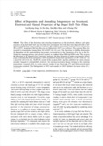
Therefore, the electro annealed films had better optoelectrical performances thanas deposited ITO films ... Transparent ITO films were deposited on a polycarbonate substrate with RF magnetron sputtering in a ... The electro annealed films demonstrated a larger figure of meritof 3.0×10⁻³Ω-1 than that of as deposited
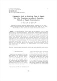
of Ag doped ZnO (ZnO:Ag) thinfilms were investigated. ... An undoped ZnO thinfilm was also fabricated at 150oC as a reference. ... The as-grownfilmdeposited at RT showed n-type conduction; however, the films deposited at higher temperatures
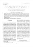
We analysed interfacial traps in organic thin-film transistors (TFTs) in which pentacene and 6,13-bis ... The thermally-deposited pentacene film consists of dentritic grains with the average grain size of around ... (triisopropylsilylethynyl)-pentacene (TIPS-pentacene) organic semiconductors were deposited by means
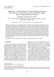
deposited onto glass substrates in a sophisticated process. ... The irradiation of a green laser was controlled during the crystallization of amorphous Si thinfilms ... A 532 nm Nd-YAG laser was applied to crystallize amorphous Si thinfilms in order to evaluate the applicability
Tungsten (W) thinfilm was deposited at 400 oC using pulsed chemical vapor deposition (pulsed CVD); ... film was then evaluated as a nucleation layer for W-plug deposition at the contact, with an ultrahigh ... It was found that resistivities of films deposited by pulsed CVD were closely related with the phases
Aluminum oxide (Al2O3) thinfilms were grown by atomic layer deposition (ALD) using a new Al metalorganic ... The as-deposited ALD-Al2O3 film was amorphous; X-ray diffraction and transmission electron microscopy ... X-ray photoelectron spectroscopy showed that the ALD-Al2O3 films deposited at 250oC were stoichiometric
Thin Film Deposition 2. ... Thin film DepositionThinFilm : Thin material layers which thickness is about 1㎛ or less than that. ... Thin film Deposition-CD(3) 1.
Thin film deposition : layers of insulators, semiconductors, and conductors form integrated circuit 등을 ... Chemical Deposition - Plating : 도금을 의미함. ... 넓은 면적에서 균일한 박막두께 증착가능 : Cathodic Arc Deposition - high power arc : Pulsed laser deposition - a high power
Conventional CVD Application of ThinFilm Technology Application of ThinFilm Technology Trend of Micro ... films ( 90nm) Electromagnetic Recording Heads Application of ThinFilm Technology {nameOfApplication ... film to be deposited.
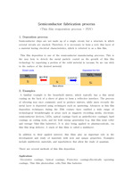
Thin film deposition is one of the semiconductor manufacturing processs. ... Advances in thin film deposition techniques during the 20th century have enabled a wide range of tolid ... which is referred to as a thinfilm.
However, when the deposition time increases, the particles forming the thinfilms are subject to a secondary ... This phenomenon indicates that the deposition time of thinfilms affects their carrier density SEM ATYPICAL ... films, with an overlapped or wrinkled form, and indicate that thinfilms growth takes place in different
Structural and optical properties of the ZnO thinfilms deposited on the ZnO buffer layers with various ... film was deposited on the ZnO buffer layers. ... We investigated the effect of ZnO buffer layer on the formation of ZnO thinfilm by ultrasonic assisted
박막증착 공정(Thin film deposition) 박막이란 얇은 막을 말한다. 박막증착 공정은 웨이퍼에 1㎛ 이하의 얇은 막을 입히는 공정이다. ... 물리적 기상증착방법 (PVD, Physical Vapor Deposition) 화학적 기상증착방법 (CVD, Chemical Vapor Deposition) 방법 가열이나 전자빔,
Li-incorporated ZnO thinfilms were deposited by using ultrasonic-assisted spray pyrolysis deposition ... In addition, the Li-incorporation changed the optical and electrical properties of the ZnO thinfilms ... To investigate the effect of Li-incorporation on the performance of ZnO thinfilms, the structural, electrical