 한컴오피스
한컴오피스 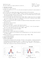
-
미리보기
목차
1. Experment procedure
2. Results and discussion
1) UV-Vis spectrometer
2) Photo counter meter
3. Reference본문내용
1. Experment procedure
A. Preperation of organic thin-film
① Prepare the glasses size in 1.5 X 1.5 cm. The glass was prepared by assistance for rapid procedure of our experiment.
② Put the glasses into plasma ashing system to make glass familiar with the solution.
③ Set the spin-coater to 25 seconds for 700RPM, 2 seconds for lamp time. And then put the glasses on the spin-coater with polymer solution by using the spuit. The color of the polymer solution turn into purple from orange Which means it turned into solid state.
④ After coat the glasses, make three different types of samples. Make six samples and each type of the samples are two pieces respectively. For the first two samples put on the hot plate for annealing. and other samples make as it is. and the other samples are pure glasses.
⑤ Prepare the solution with 1ml cuvette for measure the absorption difference between polymer in solid state and solution state.
B. Photoelectronic characterization
- Light absorption analysis
① Using UV/vis spectrometer to measure light absorption analysis.참고자료
· CBE201 Molecular engineering laboratory, KAIST, 2013.
· Introduction to polymers 3rd edition, Robert J. Young and Peter A. Lovell, CRC Press
· Polymer Chemistry 2nd edition, Paul C. Hiemenz and Timothy P. Lodge, CRC Press
· C. Ronda, Luminescence From Theory to Applications, Wiley-VCH, New York, 2008.
· Effect of Oxygen Plasma Treatment on Adhesion Improvement of Au Deposited on Pa-c Substrates, Jeong Hoon Lee, Kyo Seon Hwang and Tae Song Kim, Microsystem Research Center, Korea Institute of Science and Technology, 2004
· Pasquariello D et al 2000 Surface energy as a function of self-bias voltage in oxygen plasma wafer bonding Sensors Actuators 82 239–44
· Photoluminescence study of polycrystalline silicon thin films prepared by liquid and solid phase crystallization, S. Scho¨ nau*, J. Rappich, M. Weizman, D. Amkreutz, and B. Rech, Helmholtz-Zentrum Berlin fu¨ r Materialien und Energie GmbH, Institut fu¨ r Silizium Photovoltaik, Kekule´str. 5, 12489 Berlin, Germany태그
-
자료후기
 Ai 리뷰지식판매자가 등록한 자료는 매우 유익하고, 주제가 잘 정리되어 있어 학습에 큰 도움이 됩니다. 특히 자료의 품질이 높고, 내용이 풍부하여 많은 정보를 얻을 수 있었습니다. 앞으로도 이러한 유익한 자료가 계속 등록되기를 기대합니다!
 -
자주묻는질문의 답변을 확인해 주세요

꼭 알아주세요
-
자료의 정보 및 내용의 진실성에 대하여 해피캠퍼스는 보증하지 않으며, 해당 정보 및 게시물 저작권과 기타 법적 책임은 자료 등록자에게 있습니다.
자료 및 게시물 내용의 불법적 이용, 무단 전재∙배포는 금지되어 있습니다.
저작권침해, 명예훼손 등 분쟁 요소 발견 시 고객센터의 저작권침해 신고센터를 이용해 주시기 바랍니다. -
해피캠퍼스는 구매자와 판매자 모두가 만족하는 서비스가 되도록 노력하고 있으며, 아래의 4가지 자료환불 조건을 꼭 확인해주시기 바랍니다.
파일오류 중복자료 저작권 없음 설명과 실제 내용 불일치 파일의 다운로드가 제대로 되지 않거나 파일형식에 맞는 프로그램으로 정상 작동하지 않는 경우 다른 자료와 70% 이상 내용이 일치하는 경우 (중복임을 확인할 수 있는 근거 필요함) 인터넷의 다른 사이트, 연구기관, 학교, 서적 등의 자료를 도용한 경우 자료의 설명과 실제 자료의 내용이 일치하지 않는 경우
문서 초안을 생성해주는 EasyAI