목표 - 주어진 논리 회로에 대해 VHDL프로그램을 이용하여 설계하고 test bench를 이용하여 시뮬레이션을 하여 결과를 확인할 수 있다.1. Write a VHDL program of 74X381.2. Write a VHDL programs of 4-input, ..
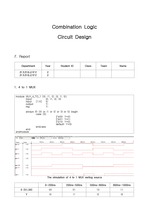
Input 은 4비트짜리 logic vector w이고 실습 조건에 따라 En도 input으로 추가하였다. Output은 16비트짜리 logic vector y이다. ... 또한 logic vector 활용법을 익힐 수 있는 실습이다. 4 to 16 VHDL Decoder의 코드는 다음과 같다. ... 이는 En과 w를 연결한 5비트짜리 logic vector 이다. y의 값은 Enw 값에 매칭되는 w 값이다.En이 ‘0’일 때 F는 무조건 ‘0’이다(0 when others)
가. 실험목표-HDL 문법을 활용하여 Verilog 설계 및 시뮬레이션을 할 수 있다.-감산기와 비교기의 구조 및 동작을 이해 및 확인한다.나. 실험결과1.Full Subtractor아래 그림은 예비보고서에서 설계했던 전감산기(FS)의 시뮬레이션 결과이다. testbe..
가. 실험목표-HDL 문법을 활용하여 Verilog 설계 및 시뮬레이션을 할 수 있다.-Decoder, Encoder, MUX의 구성과 작동 방식을 이해 및 설계한다.나.실험결과1.2-bits 2:1 MUXFig.1.은 2-bits 2:1 MUX의 시뮬레이션 결과이다...
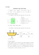
Pre - Report Combination Logic Circuit Design Department Year Student ID Class Team Name 전기전자공학과 2 2007142123 ... The 2x1 multiplexer is data selective logic circuit because it outputs one input selected from two inputs ... Decoder> -Decoder Decoder can take the form of a multiple-input, multiple-output logic
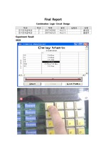
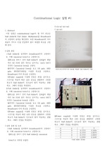
Final Report Combination Logic Circuit Design 학과 학년 학번 분반 실험조 성명 전기전자공학과 2 2007142082 thu1-5 홍성현 전기전자공학과 ... So in order not to using the Logic gates, we should use a 32×1 multiplexer because the 32×1 mux can permit
Post-Lab Report Lab#04 CombinationalLogic Design 1 @ Arithmetic Logic and Comparator 담당 교수 강 상 혁 담당 ... Purpose of this lab Verilog HDL을 통하여 CombinationalLogic Circuit을 설계한다. 나. ... Essential Backgrounds 1) Combinational Circuit의 정의 조합회로는 어떤 시점에 대해서도 출력값이 그 시점의 입력값으로 정해지는 논리 회로를 의미하는데
Purpose of this lab Verilog HDL을 통하여 CombinationalLogic Circuit을 설계한다. 나. ... Post-Lab Report Lab#05 CombinationalLogic Design 2 @ Decoder, Encoder and Mux 담당 교수 강 상 혁 담당 조교 실 험 ... Methods 1) 3:8 Decoder Logic design 가) 프로젝트를 생성한다.
Pre-report Combination Logic Circuit Design Department Year Student ID Class Team Name EEE 2 2009142104 ... In digital electronics, a decoder can take the form of a multiple-input, multiple-output logic circuit ... In digital electronics, a decoder can take the form of a multiple-input, multiple-output logic circuit
CombinationalLogic Design Using FPGAs ◆Introduction Through this experiment, I get familiar with the ... I also learned how to design simple combinationallogic circuits and how to synthesize my design. ... -Lab work Verilog Code module lab1_1(a,c,f); input a,c; output f; assign f= a|c; endmodule [Figure1_Logic