majority carrier injection (diffusion) to the opposite side of the junctionminority carriers wandering into the depletion region and being accelerated..
crystalline material has the same atomic patttern or order throughout the maaterial, whil polycrystalline material has crystalline subsections that ar..
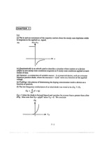
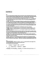
(a) Under the quasistatic assumption the carriers and hence the device under analysis are assumed to respond to a time-vaying signal as if it were a d..
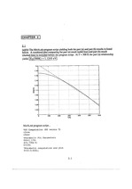
the matlab progran scripy yielding both the part (a) and part (b) results is listed below. a comined plot comparing the part (a) result (solid- line)..
the in and out movement of the majority carriers about the steady-state depletion width in response to the applied a.c. signalvaractor - a contraction..
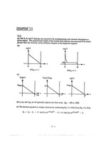
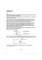
(f) In the vicinity of the drain under operational condition, channel carriers, and carriers entering the drain depletion region from the substrate, p..
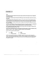
18.1(a)In theory the two quantities are numerically identical.(b)The MOS-C or MOSFET under test is heated to an elevated temperature and a bias is app..
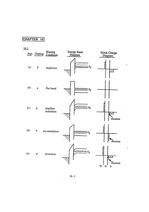
17.1(a) Carriers enter the channel at the source contact and leave the channel(or are "drained") at the drain contact.(b) Channel...inversion layer be..
15.1(a)Field Effect....modulation of the semiconductor conductivity vy an electric field applied normal to the surface of the semiconductor.(b) Channe..
reason : in intrinsic material the scattering is due ezclusively to lattice scattering in heavily doped materials ionized impurity scattering is also ..
14.1(a)MS, Schottky, and Hot Carrier are just alternative names for a rectifying metal-semiconductor contact, Hot Carrier diodes are typically small a..
좋은 도체나 부도체를 반도체라고 부른다. ■ 다이오드 동작원리 - 실리콘에 각각 도핑하여 P형 반도체와 N형 반도체를 접합하게 되면 P형의 정공과 N형의 전자가 접합부에서 결합하여 ... 반도체에 대한 소개) ※ 단원목표 - 반도체 다이오드의 직류특성과 SEMICONDUCTOR DEVICE 회로 보드를 통한 작용을 확인한다. ※ 단원 기본 지식 ■ 다이오드 - 다이오드 ... 회로 위치와 인지 ▶ 반도체 회로 보드 - 8개의 회로 블록으로 이루어져 있다. ① 다이오드와 반파 정류 ? 두 개의 저항, 다이오드가 있다. ?