..PAGE:1 디자이너는 의미를 생산하는가? 저자로서의 디자인 2반 최광우, 이지원 ..PAGE:2 Post-Modernism 진정한 독창성-선별적 차용과 인용 ..PAGE:3 Roland Barthes, 글쓰기-인용들의 짜임 다양한 인용들의 의미 선택의 주체=독자..
Cmos process design rules The design rules are usually described in two ways : 2. ... Cmos process design rules ■ Cmos design rules : The physical mask layout of any circuit to be manufacture ... Semiconductor Device and Design - 7 KwangWoon University Contents 1. CMOS process design rules 2.
전장 설계직무의 업무에 임하게 된다면, 설계 tool 습득과 정해진 designrule에 맞춰 설계할 수 있는 능력이 필요하다고 생각합니다. ... 또한, layout을 통해 회로 내부 소자들의 전기적인 연결이 어떻게 이루어지는지 보았고 회로 설계는 정해진 designrule이 있어 이에 맞게 물리적 배치와 배선하는 설계 해야
Recent Advances in Bulk Heterojunction Polymer Solar Cells -New Materials and Design Rules- 1 Contents ... New Materials and Design Rules for Efficient Light Harvesting - Donor Polymers Developed at Early Stage ... Charge transport and collection 5 New Materials and Design Rules Solar energy Concentrated in visible
빠르게 검사하기 위해 resistance reflection rule을 사용한다. ... Design2 최대전압 이득을 얻기 위한 회로 구현 Show the detailed design procedures and results. ... 소신호등가회로에서 계산한 값과 resistance reflection rule로 검산한 값이 0.01차이로 거의 일치한다.
- 활성모드 -1) E-B 순방향이기 때문에 전자가 B로 넘어간다.-> 이때, 몇몇 전자는 B의 정공과 결합한다.2) C-B 역방향으로 인해 전기장이 형성되고, 그 힘으로 B로 넘어온 전자가 C로 빨려 들어간다.: ‘매우 낮은 B 전류를 가지고 C와 E 간의 전류를 조..
on an overview of the privacy protection legislation in China, this article attempts to describe the rules ... concern, and some recommendations are proposed by countries or international organizations, like privacy design
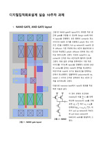
최대한 작은 공간에 gate를 구현할 수 있도록 Designrule에 따라서 layout을 진행했다. ... 따라서 이전 실습에서 다루었던 내용을 바탕으로 designrule을 참고해 rule을 어기지 않으면서 최소한으로 공간이 사용될 수 있도록 고민을 많이 했다. ... NAND gate의 layout 작성과 마찬가지로 최대한 작은 공간에 inverter를 구현할 수 있도록 designrule에 따라 layout을 진행했다.
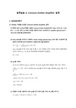
(E) 이론부의 rule of thumb in Design을 적용하여 VE를 구하고 VB와 RE를 구하라. ... Rule of thumb in Design에 의해 collector bias 전압 Vc는 collector와 emitter 사이의 전압 VCE와 emitter bias 전압 VE가 ... 같은 값을 갖도록 하면 BJT가 active region에서 동작하므로, (Active region; ) (F) 이론부의 rule of thumb in Design을 적용하여 R1,
(F) 이론부의 rule of thumb in Design을 적용하여 , 를 구하라. ... (E) 이론부의 rule of thumb in Design을 적용하여 를 구하고 , 를 구하라. 이다. 이고, 이다. ... 이 값을 이용하여 설계한 CE amplifier의 입력저항 을 구하라. (1차 설계 완료) Rule of thumb in Design을 적용하면 에 흐르는 전류 는 collector에
He was both admired and criticized throughout the world during his rule. ... De Kock took responsibility for murdering and torturing dissidents opposed to white-only rule. ... 지명, 지정/The district is under consideration for designation as a conservation area. 15. legislation 법률
(E) 이론부의 rule of thumb in Design을 적용하여 를 구하고 와 를 구하라. rule of thumb in design에 의하면 경험적으로 == 로 설계하면 BJT가 ... (F) 이론부의 rule of thumb in Design을 적용하여 , 를 구하라. ... 이 값을 이용하여 설계한 CE amplifier의 입력저항 을 구하라.(1차 설계 완료) rule of thumb in design에 의하면 경험적으로 에 흐르는 전류 은 의 이 되도록
(F) 이론부의 rule of thumb in Design을 적용하여 R _{1} , R _{2} 를 구하라. ... 이론부의 rule of Thumb in Design를 참고한다. : 경험에 의하면 Collector 바이어스 전압 V` _{`C} `는 collector와 emitter 사이의 전압 ... 이 값을 이용하여 설계한 CE amplifier의 입력저항 R _{i`n}을 구하라. (1차 설계 완료) rule of Thumb in Design : 경험에 의하여 R _{1} 에
article 33, Clause 1 of Information Industry Promotion Act and Article 11, Clause 1 of its Enforcement Rule ... CERTIFICATE of Designation as a Knowledge Information Security Consulting Service Provider for Information ... Infrastructure Name of Service Provider: Name of Representative: Address: Validity Period of Designation
Vc = Vcc – IcRc = 12 – 1*5 = 7 V 이론부의 rule of thumb in Design을 적용하여 VE를 구하고 VB와 RE를 구하라. ... Rule of thumb in Design에 따르면 Collector 와 emitter 사의 전압 VCE 와 emitter bias 전압 VE가 같은 값을 갖도록 하면 BJT가 active ... 이 값을 이용하여 설계한 CE amplifier의 입력저항 Rin을 구하라. (1차 설계 완료) Rule of thumb in Design 을 적용하면 R1에 흐르는 전류는 collector에